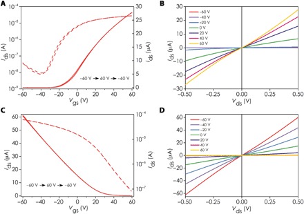
Fig. 4. Negligible hysteresis of the doped p/n-type MoTe2 transistor.

Transfer characteristic curves of device B at Vds = 500 mV after intense n-type doping (A) and p-type doping (C). The sweeping directions were from −60 to +60 V in the positive direction and +60 to −60 V in the negative direction. The sweeping rate of Vgs was 1.2 V/s. Corresponding output characteristic curves at Vgs = −60, 60, −40, 40, −20, 20, and 0 V of the n-doped (B) and p-doped (D) MoTe2 FETs.
