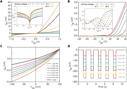
Fig. 5. Direct writing of a stable p-n junction and optoelectronic applications.

(A) Output characteristic curves of device C at Vgs = 0 V after different photoinduced doping at writing voltage = 0, 5, 10, 20, 30, 40, 50, and 60 V. (B) Transfer characteristic curves of device C at Vds = 500 mV after photoinduced modulation doping. (C) Output characteristic curves of the device under light illuminations of different powers. (D) Photo-switching characteristics of the device during multiple illumination cycles. Vds = 0 V and Vgs = 0 V.
