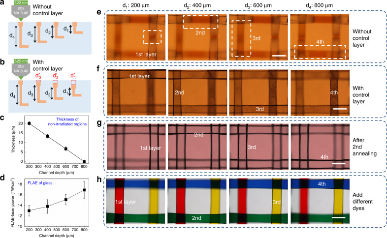
Fig. 2.
Fabrication of a 3D multilayered microchannel structure with optimized parameters. Schematic illustration of the fabrication for four-layered microchannels without (a) and with (b) control layers. c Thickness of the control layer (nonirradiated regions) in FLAE as a function of the channel depths to form at different layers (1–4 layers). The thickness is ~15, ~10, ~5, and ~0 μm for the 1st, 2nd, 3rd, and 4th layer channels, respectively. d Relationship of the FLAE laser power and channel depth. The laser powers required for the 1st, 2nd, 3rd, and 4th layer channels are 13±1, 13.8±1.3, 15.08±1 and 16.9±1.56 TW/cm2, respectively. Generally, a deeper channel requires more laser power. e Optical microscopy image for the four-layered microchips after HF etching without a control layer. A deeper depth corresponds to longer unetched areas. f Optical microscopy image for the 4-layered microchips after HF etching with the control layer. All four layers can be simultaneously completely etched. g Optical microscopy image for the 4-layered microchips with high smoothness after the second annealing. h Four-layered channels arranged in parallel crosses at depths of 200, 400, 600, and 800 μm by FLAE and filled with red, green, yellow, and blue dye solvents. The four solvents do not mix, which verifies that each layer is well isolated. Scale bars: 200 μm

