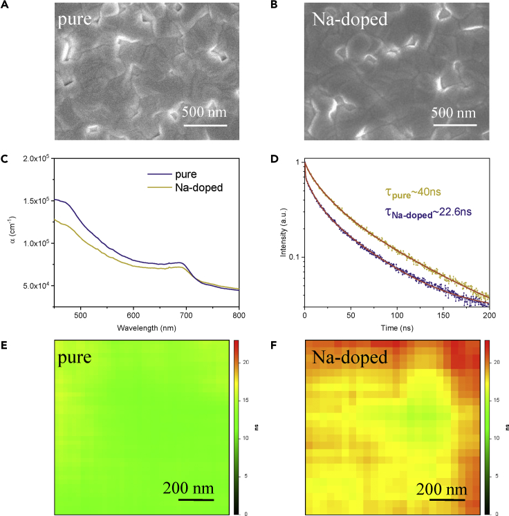
Figure 4.
Morphology and Optoelectronic Properties of CsPbI3 and Cs0.95Na0.05PbI3 Films
(A and B) Top-view SEM images of (A) CsPbI3 and (B) Cs0.95Na0.05PbI3 films.
(C–F) (C) Absorption coefficient (α) versus wavelength curves and (D) TRPL of CsPbI3 and Cs0.95Na0.05PbI3 films. Fluorescence lifetime mapping images of (E) CsPbI3 and (F) Cs0.95Na0.05PbI3 films.

