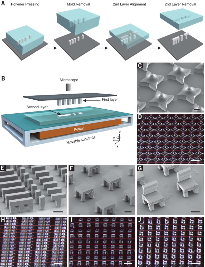
Fig. 1.
Assembly of 3D microstructures using the SEAL process. (A) Microstructures are fabricated by pressing and heating polymer into a patterned PDMS base mold and delaminating these structures onto a substrate to create the first layer. A second layer is then formed by using a similar molding process against a Teflon surface, which allows the features to remain in the PDMS mold after cooling. The second layer is aligned, placed into contact with the first layer, and sintered by using a mild heating step. (B) Schematic depicting the alignment and sintering equipment, consisting of a mask aligner retrofitted with a Peltier heater. A glass slide containing the first layer is suspended upside down from a fixed mask holder by means of a vacuum while the second layer, still in the PDMS mold, is placed on the wafer chuck, aligned using the stage rotation and translation knobs, put into contact, and heated until they fuse.This approach can be used to create a variety ofmicrostructures, including (C and D) stars, (E and H) letters spelling “MiT,” (F and I) two-layered tables, and (G and J) three-layered chairs. Scale bars indicate 200 mmfor scanning electron microscopy (SEM) images and 1mmfor optical images.Optical images were stitched together from multiple images to enable a better depth of focus.The interfaces between images are denoted by thin red lines.

