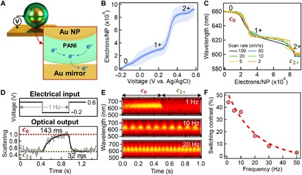
Fig. 4. Electrical and optical switching dynamics of eNPoM nanopixels.

(A) Schematic of electron transfer from PANI to Au mirror through the gap. (B) Charge flow per nanoparticle in the gap of each eNPoM versus applied potential. (C) Optical dynamics of coupled plasmon mode versus number of electrons transferred at the gap. (D) Square-wave modulation of the applied potential at 1 Hz (top) and associated normalized scattering intensity (bottom) of single eNPoM at wavelength of c0 peak, showing dynamics for reduction (143 ms) and oxidation (32 ms). (E) Reversible optical switching of an eNPoM under square-wave modulation at 1, 10, and 20 Hz. (F) Switching contrast of eNPoM versus applied modulation frequency.
