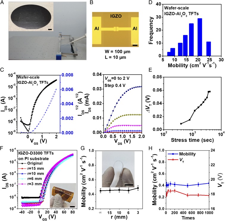
Fig. 5.
Scalable CBC fabrication of high-performance IGZO TFTs on both high-k Al2O3 dielectrics and low-k polymer dielectrics. (A) Photo of the BC process; Inset shows blade-coated devices on a 4-inch Si wafer. (Scale bar, 1 cm.) (B) Optical image of a patterned low-voltage IGZO TFT. (Scale bar, 100 µm.) (C) Transfer (Left) and output (Right) characteristics of low-voltage CBC IGZO TFT on high-k Al2O3 dielectrics. The annealing time for both IGZO and Al2O3 layers is 60 s. (D and E) Distribution of saturation mobilities (D) and ΔVT vs. time (E) of CBC/FA-CS-derived IGZO TFTs on P-FA-CS Al2O3/Si substrates (VGS = +1.0 V). (F and G) Transfer curves (F) and mobility variation (G) of top-gate flexible CBC/IGZO TFTs on a PI substrate as a function of bending radius. (Inset) Photo of device under bending. (Scale bar, 1 cm.) (H) Mobility and threshold voltage stability for bending test cycles with a radius of 6 mm.

