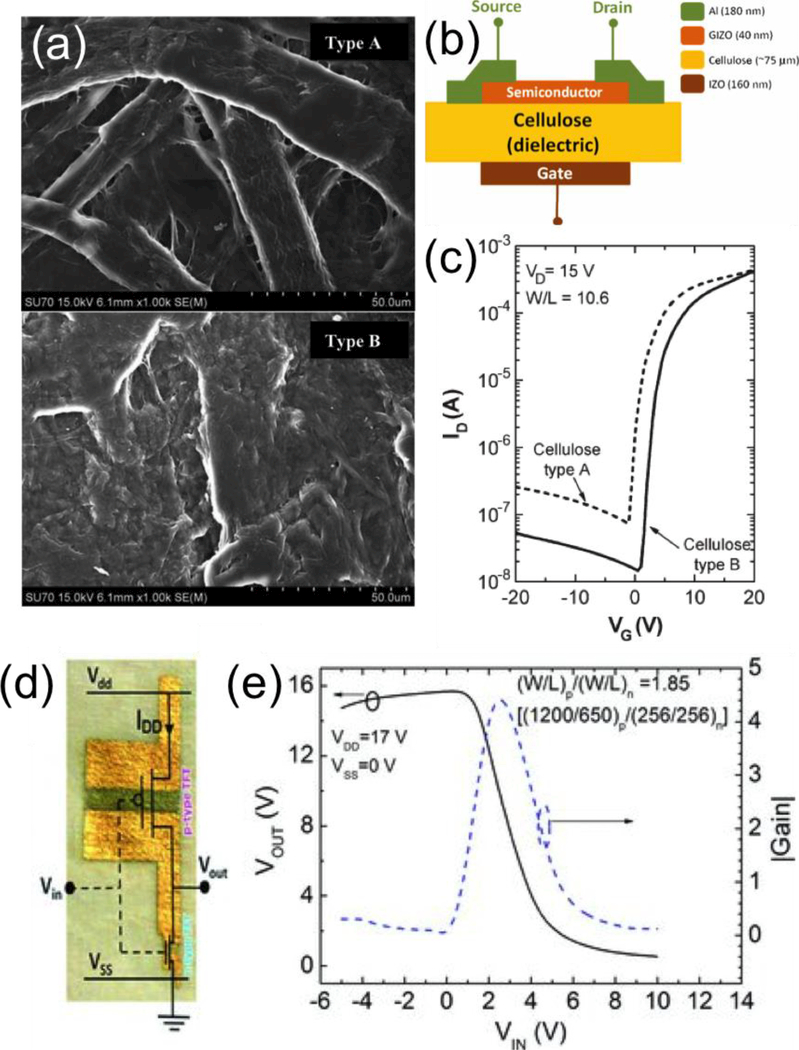
Figure 5.
(a) SEM images showing two different types of papers. Type A has more porous cavities while type B is highly packed. (b) Schematic of the field effect transistor using cellulose paper as a gate dielectric. (c) I-V transfer characteristics measured at saturation region (drain voltage of 15 V) for devices with two different types of papers. Measurements are conducted at room temperature. Reproduced with permission.[94] Copyright 2008, Institute of Electrical and Electronics Engineers. (d) An image showing paper-based CMOS inverter with p-type TFT (a gate width to length (W/L) ratio of 21.8) and n-type TFT (W/L ratio of 11.8). (e) Device transfer characteristic of the paper-based CMOS inverter with the corresponding gain. Reproduced with permission.[93] Copyright 2013, Wiley-VCH.

