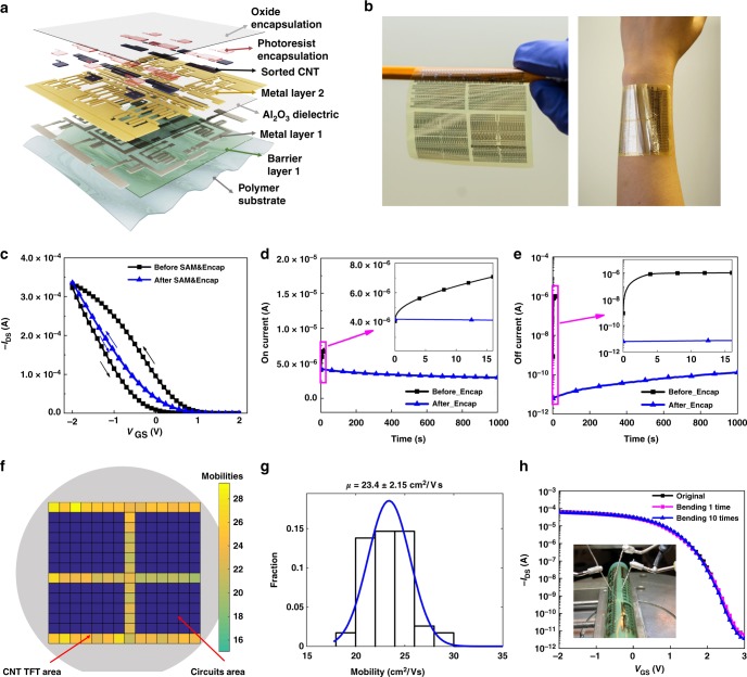
Fig. 2.
Device layer structures and electrical characterizations of CNT TFTs on a plastic substrate. a Layer structures of the CNT TFT device. b Photos of CNT TFT devices fabricated on a 10-μm flexible polyimide substrate. The thin flexible devices show good conformal attachment to human skin. c Transfer characterizations of CNT TFTs before and after SAM layer modification and Al2O3 encapsulation (VDS = −1 V). d On-current bias stability of a CNT TFT before and after Al2O3 encapsulation. Inset shows the enlarged area (0–16 s) of the bias stability test. e Off-current bias stability of a CNT TFT before and after Al2O3 encapsulation. Inset shows the enlarged area (0–16 s). f, g Mobility statistics from 56 CNT TFTs tested on a 4-inch wafer. The 56 CNT TFTs are distributed on the yellow areas. The colored scale bar indicates the mobility values. Dark blue areas are circuit areas and were not tested. The average mobility of CNT TFTs is 23.4 cm2 V−1 s−1 with a standard deviation of 2.15 cm2 V-1 s-1. h Bending test of a flexible TFT with a bending radius of 5 mm. Only slight current changes (<10%) were observed after 10 times of repeated bending. Inset shows the bending and testing setup image

