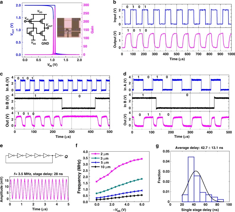
Fig. 3.
Flexible pseudo-CMOS combinational logic gates and ring oscillators. a Circuit diagram of using depletion-mode TFTs, die photo, input–output characteristics and small signal gain of a pseudo-CMOS inverter. Channel length (L) = 10 μm, VDD = 2 V, VSS = −3 V. b Measured waveforms of a pseudo-CMOS inverter running at 10 kHz. L = 10 μm, VDD = 2 V, VSS = −3 V. c Measured waveforms of a pseudo-CMOS NAND gate running at 20 kHz. L = 10 μm, VDD = 3 V, VSS = −3 V. d Measured waveforms of a pseudo-CMOS XOR gate running at 10 kHz. L = 10 μm, VDD = 3 V, VSS = −3 V. e Circuit diagram and output characteristics of a five-stage ring oscillator. The ring oscillator shows an oscillation frequency of 3.5 MHz with a stage delay of 28 ns. L = 2 μm, VDD = 3 V, VSS = −3 V. f Frequency responses of the five-stage ring oscillators under various VSS voltages and with different channel lengths. VDD = 3 V. g Stage delay statistics of a total of 44 five-stage ring oscillators with VDD = 3 V, VSS = −3 V. The five-stage ring oscillators show average stage delays of 42.7 ± 13.1 ns, comparable to current state-of-the-art CMOS-type CNT circuits7. Note: Results of 2 µm ring oscillators in e and f are from different devices and they are slightly different in performance due to process variations as shown in g. For measurement data in e, due to a large loading effect (measured to be ~125 pF), the measured waveform only has ~10 mV scale, which is also consistent with our simulation results in Supplementary Fig. 15

