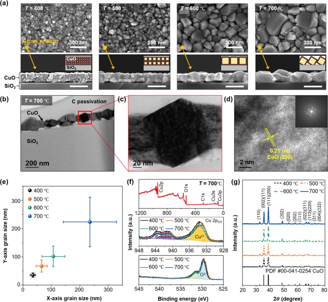
Figure 3.
Material property of the fabricated CuO nanofilm. (a) Surface SEM images (upper panels) and cross-sectional SEM images (lower panels) of the CuO nanofilms annealed at 400, 500, 600, and 700 °C, respectively. Insets of lower panels show cross-sectional schematics of the CuO nanofilms. (b) TEM image, (c) Magnified TEM image, and (d) HRTEM image of the CuO nanofilm annealed at 700 °C. (e) Measured grain sizes, (f) XPS spectra results (top: wide-scan spectrum, middle: spectra for Cu 2 p, bottom: spectra for O1 s), and (g) XRD results of the nanofilms annealed at various annealing temperatures.

