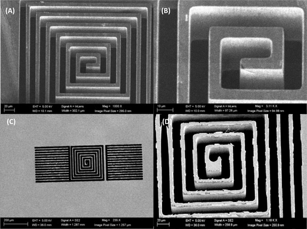
Figure 2:
SEM images of the stencil wafer. Top view of the six turns single layer planar spiral coil (A), zoomed in view of the coil from the front (B), overview of the entire coil structure from the back side (C) after flipping the stencil wafer over showing that the DRIE reached through and through, and details of the back side of the stencil wafer that show a bottom footing (D).

