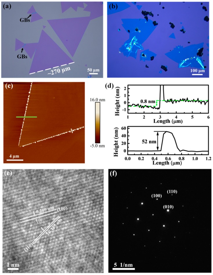
Figure 2.
Representative optical images of the as-grown WS2 flakes on the covering (a) and bottom (b) SiO2/Si substrates, respectively. AFM image (c) and its corresponding height profiles (d) of an equilateral triangular WS2 flake on SiO2/Si substrate. High-resolution TEM image (e) and its corresponding SAED pattern (f) of the as-grown triangular WS2 transferred on a holy carbon-coated copper TEM grid.

