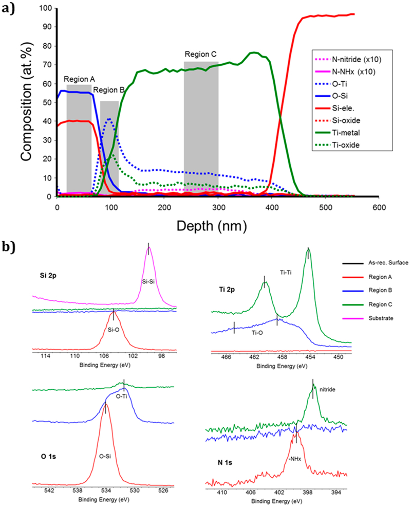
Figure 3.
XPS analysis of elemental composition through the thickness of the device from Figure 2a. (a) Depth scale determined by a sputter rate of 15 nm/min. Sputter cycles were 30 s. Shaded areas show particular regions that had different chemical signals, i.e., N was present in the SiO2 layer in e chemical form and was present in a different chemical form in the Ti layer. (b) Individual spectra from these regions are compared for Si, O, Ti, id N. Note that the N (NHx and nitride) signals are all plotted magnified by a factor of 10.

