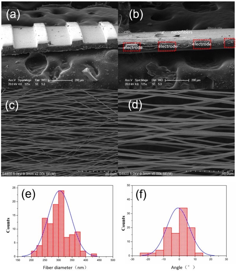
Figure 2.
(a) SEM image of the flexible parallel copper electrode, (b) side view SEM image of the P(VDF-TrFE) nanofibers and electrode after electrospinning process, (c) top view SEM image of the nanofibers, (d) enlarged SEM image of the nanofibers, (e) typical fiber diameter distribution statistics, (f) fiber orientation distribution statistics.

