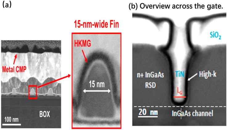
Figure 31.
Cross-section images of the self-aligned InGaAs-OI FinFET architecture where (a) the scaled HKMG deposited on a 15-nm-wide fin using a highly conformal and uniform PEALD* process [192], and (b) shows CS STEM images across the gate showing the InGaAs FinFET with Lg = 13 nm [194]. * plasma-enhanced atomic layer deposition.

