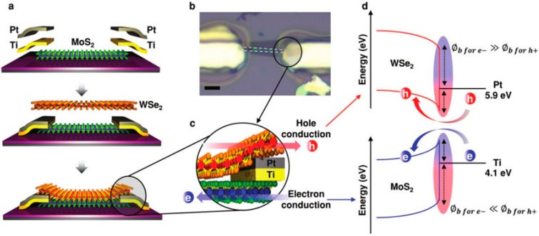
Figure 33.
(a) Schematic of fabrication, a WSe2/MoS2 hetero-structure dual-channel FET. (b) Optical picture of a processed transistor. The dashed line shows the bottom MoS2 layer, (c) schematic of electron and hole transport in one channel of dual-channel FET, and (d) band diagram WSe2-Pt metal (top) and MoS2-Ti. The symbol ϕb in the picture stands for the barrier for hole and electrons [206].

