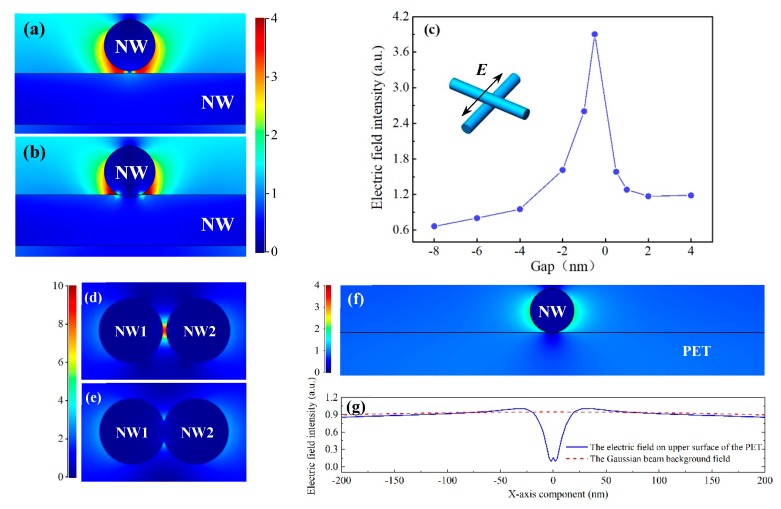
Figure 3.
Simulated cross-sectional electric field distribution in the adjacent of two perpendicularly crossed AgNWs at the gap of (a) 2 nm and (b) −2 nm, respectively. (c) Field intensity in the intersection area at different gap distances calculated for the structures in the inset. The polarized direction of laser is perpendicular to the top nanowires (black arrow). Negative values on the x axis correspond to interpenetrating nanowires. Simulated electric field distribution between a pair of parallel AgNWs with at the gap of (d) 2 nm and (e) −2 nm, respectively. (f) Electric field distribution between nanowire and PET surface. (g) Line plot of the x component of the electric field (blue line) on upper surface of the PET and the Gaussian beam background field (red line).

