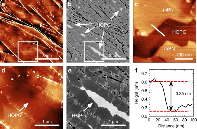
Fig. 1.
Surface morphology of epitaxial monolayer BN on graphite. Atomic force microscopy (AFM) of mBN grown on HOPG (boron cell temperature TB = 1875 °C, growth temperature Tg = 1390 °C and growth time of 3 h). a Large-area AC-mode AFM topography of mBN growth on HOPG: the brighter (i.e. topographically higher) regions are due to 3D aggregates of hBN at HOPG step edges. b Phase-channel data for image a: the white arrows indicate regions of exposed HOPG, uncovered by hBN growth. c Small area contact-mode AFM image of the mBN boundary next to an exposed region of HOPG, showing the characteristic monolayer BN step height. d Zoom of the region indicated by the white box in a. e Phase-channel image for image d. f Line-profile along the interface between mBN and exposed HOPG as indicated by the white line in image c showing the characteristic monolayer BN step height

