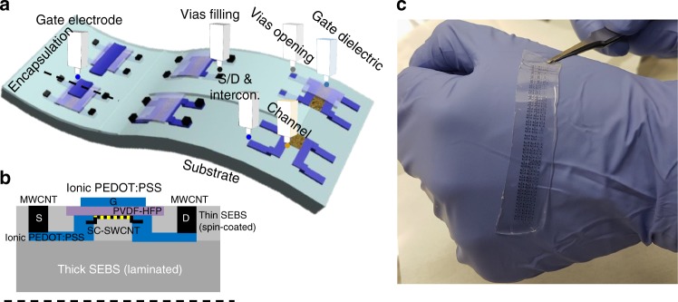
Fig. 1.
General concept and design. a Sketch of the intrinsically-stretchable array of transistors representing how each active material of the transistor was additively fabricated with the same inkjet (IJ) printing method. These materials were used to form: source (S), drain (D), and gate (G) electrodes, source and drain interconnections, gate dielectric, channel, and through encapsulation vias. The dashed line corresponds to the location of the cross-section shown in b. b Sketch of the cross-section of a device, where the each layer material is labeled. c Picture of an array of transistors IJ printed over a large area and bent over a hand

