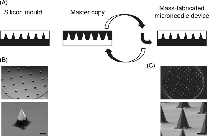
Figure 1.

Production process and finished microneedle arrays made from COP. A schematic layout of the mass‐fabrication process used for the microneedle devices in this study can be seen in (A). Brightfield microscopic images of microneedle arrays in silicon are seen in (B). (C) Shows a brightfield microscopic image of an exemplary microneedle array in COP and a detailed electron microscopic image of an exemplary needle in COP. Scale bars equal 200 μm.
