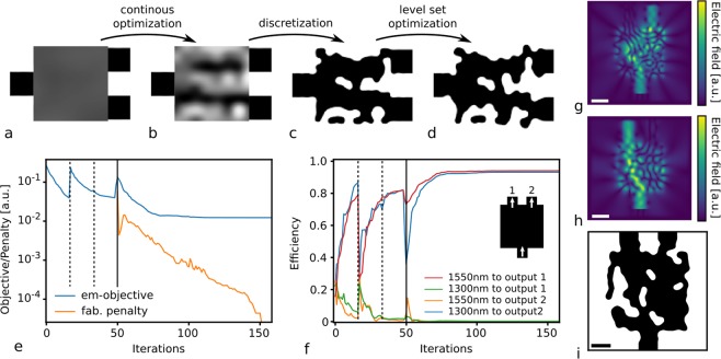
Figure 3.
Inverse design method (a–d): (a) random initial condition for a waveguide demultiplexer, (b) structure after optimization in continuous stage, (c) structure after discretization step, (d) structure after optimization with a level set parametrization and fabrication constraints. WDM optimization with fabrication constraints (e–i): (e) EM-objective (fEM) and fabrication penalty (ffab) at every iteration, (f) coupling efficiency at every iteration. The dotted vertical line in a and b indicates a change in the sigmoid function slope (Suppl. Information). The full vertical line indicates the continuous-to-discretization step. (g,h) Electric field intensity of the final structure at 1300 nm and 1550 nm wavelength, respectively, and (i) final structure. The scale bar in (g–i) is 0.5 μm.

