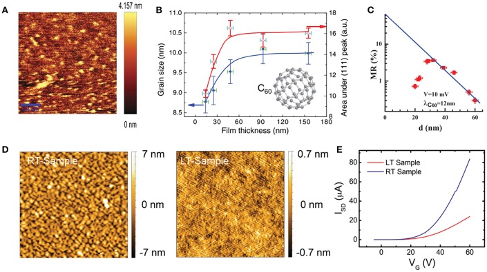
Figure 3.
The effect of morphology on carrier mobility and spin transport distance. AFM image of C60 thin film (A). The relationship between grain size and film thickness, and the area of (111) Bragg scattering peak and film thickness (B). C60 thickness dependence of MR with bias of 10 mV (C). [A&B&C reproduced from (Nguyen et al., 2013), with permission of American Physical Society] AFM images of F16CuPc fabricated at RT and LT (D). Transfer curves of F16CuPc-based OFET at RT and LT (E). [D&E reproduced from (Sun X. et al., 2016), with permission of John Wiley and Sons].

