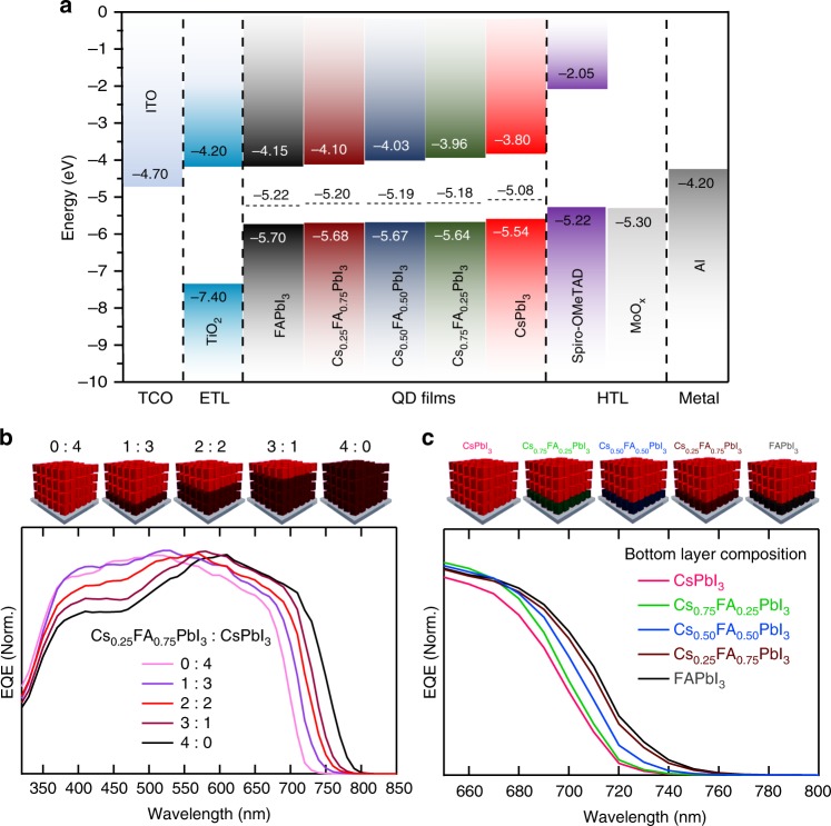
Fig. 2.
Optical and electronic properties of perovskite QD heterojunction. a Energy band positions for perovskite QD compositions and contact layers considered in this work. The Fermi level positions (denoted by horizontal dotted lines) and valence-band edges (Ev) of all perovskite QD films were determined by UPS and XPS, respectively. The conduction band edges (Ec) were calculated by adding the bandgap energy26 to Ev for the corresponding perovskite QD films. b EQE spectra of solar cells with varying thickness ratio of the Cs0.25FA0.75PbI3 layer to CsPbI3 layer in the perovskite QD absorber. c EQE spectra of solar cells with different compositions of the bottom layer in the perovskite QD absorber where the thickness ratio of the mixed-cation CsxFA1–xPbI3 QD layers to CsPbI3 QD layers is 1:3 in all cases

