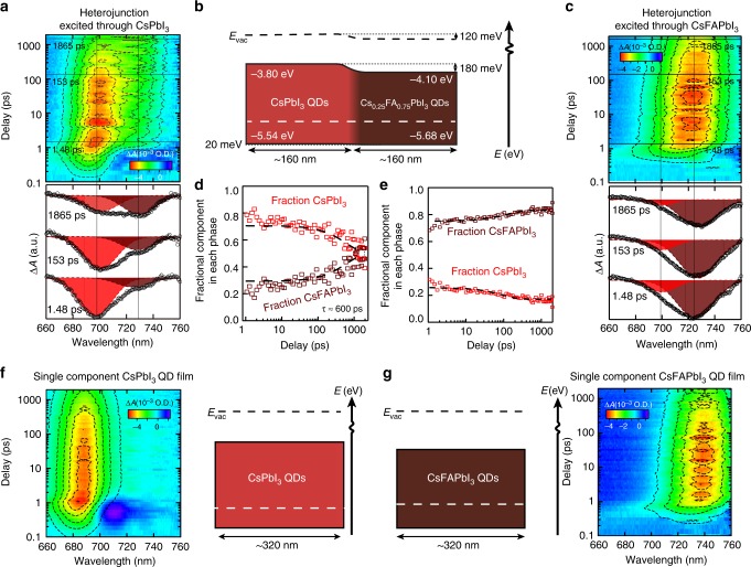
Fig. 4.
Transient absorption of heterojunction QD films. a Pseudocolor image of transient response for QD heterostructure when photoexciting through the CsPbI3 layer. For each of the surface plots with dashed contour lines one can visualize the carrier populations at various delay time delays between the pump and probe beam with the model described. Select cuts through the data are presented below the surface plots and offset vertically for clarity. Cuts are shown at 1.48 ps, 153 ps, and 1865 ps time delay. The spectra at each delay can be represented by the bleaching of two Gaussian peaks, one has a center wavelength at 697 nm (red-shaded Gaussian) and is associated with carriers occupying CsPbI3 while the other peak has a center wavelength at 728 nm (brown-shaded Gaussian) and is associated with carriers spatially occupying the Cs0.25Fa0.75PbI3 component. Vertical lines show the position of the two centered components. b Energy level diagram of the heterostructured film with estimated band alignment from UPS. In experiment a light impinges from the left (CsPbI3 QDs) while for c light impinges from the right (Cs0.25FA0.75PbI3 QDs). From the alignment, electrons are driven to the FA-containing side with a conduction band offset of 180 meV while holes have a small (20 meV) offset driving holes toward CsPbI3 c Pseudocolor image of transient response for QD heterostructure when photoexciting through the Cs0.25FA0.75PbI3 layer. The coloring scheme of the decomposed spectra is the same as in a. d, e The decomposed fraction of the TA signal for each delay measured that arises from the CsPbI3 (red-squares) and Cs0.25FA0.75PbI3 (brown-squares) as a function of time when photoexciting through CsPbI3 (d) or through Cs0.25FA0.75PbI3 (e). For d, the fraction of CsPbI3 decreases over time while Cs0.25FA0.75PbI3 increases as electrons are transferred into the FA-containing layer with a charge transfer time average of around 600 ps. For e, the fraction of CsPbI3 and Cs0.25FA0.75PbI3 is analyzed after the first ps and then stay relatively unchanged. f Pseudocolor image (left) and diagram (right) of a thick single component CsPbI3 film g Pseudocolor image (right) and diagram (left) of pure Cs0.25FA0.75PbI3

