Figure 4.
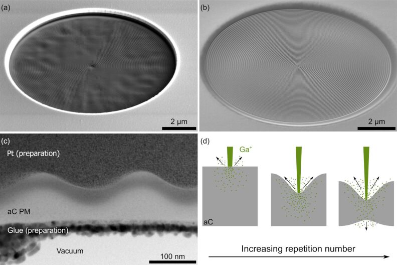
SEM images after structuring the pattern according to Equation 3 with kρ = 10 µm−1 for (a) a FIB-prepared and (b) a floated aC thin film. Since the latter is smoother, the sinusoidal structure has a better quality. (c) The generated sinusoidal structure is visible in the bright-field TEM image of a cross-section lamella of a PM with kρ = 5 µm−1. Pt was deposited on top to protect the structure during TEM lamella fabrication. We stabilized the free-standing thin films for the lamella preparation by filling the pyramid-shaped trenches with glue. (d) The scheme presents a possible explanation for fast hole formation towards the end of the pattern milling process. The middle scheme corresponds to the situation shown in (c).

