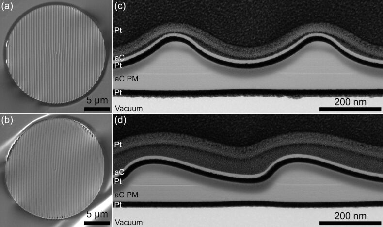
Figure 5.
Top-view SEM images of (a) a sinusoidal and (b) a saw-tooth-shaped holographic PM for the generation of VBs. The aC thin films in both images show slight bulging. In (b) holes near the PM edge are visible. Bright-field TEM images of cross-section samples from the (c) sinusoidal and (d) saw-tooth shaped thickness profiles reveal the thickness offset and implanted Ga similar to Figure 4c.

