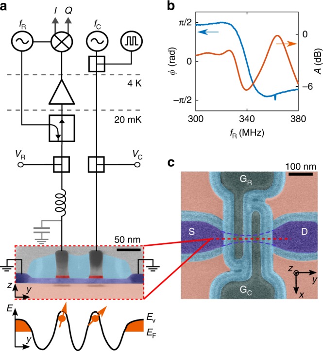
Fig. 1.

Device layout and circuitry for qubit dispersive sensing and manipulation. a False-color transmission electron micrograph of a double-gate Si device. The 11-nm-thick, 35-nm-wide Si nanowire (light blue) connects p-type, boron-doped source-drain contacts (dark blue) and lies on a 140-nm-thick SiO2 buffer layer (pink). The two 35-nm-wide gates (grey) are spaced by 35 nm. Si3N4 spacers (cyan) prevent dopant implantation in the Si channel. At 20 mK, proper gate voltages induce the accumulation of two hole quantum dots: one can be used as a spin qubit, the other as a helper dot for qubit readout. One gate is connected to a lumped-element resonator excited at frequency fR for dispersive readout. A ultra-high frequency digital lock-in demodulates the reflected signal after a directional coupler, separating the incoming and outgoing waves, and a low-noise amplifier at 4 K. The other gate applies square pulses and GHz radiation to drive controlled coherent rotations of the hole spin qubit. At the bottom, DQD energy diagram with Ev as valence band edge and EF as Fermi energy. b Phase response (ϕ) and attenuation (A) of the resonator at base temperature. c Scanning electron micrograph of the device
