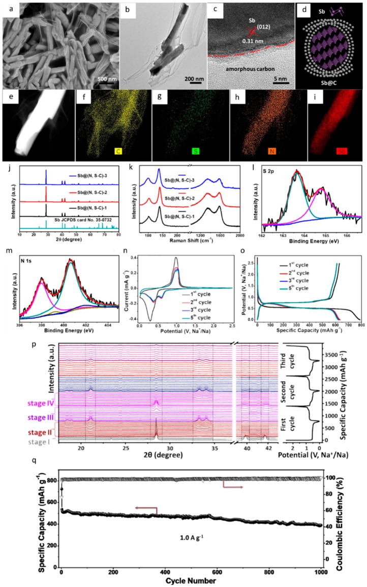
Figure 3.
Structural characterization and electrochemical performance analysis of Sb-based alloy (Sb@(N, S−C)) as an anode in SIBs: (a) SEM image of Sb@(N, S−C)-2. (b) TEM image of Sb@(N, S−C)-2 shows Sb nanorod diameter (120–160 nm). (c) HRTEM image of Sb@(N, S−C)-2 reveals the amorphous carbon and clear lattice corresponding to the plane (012) of Sb. (d) Schematic representation of Sb@(N, S−C)-2. (e–i) Elemental mapping of Sb@(N, S−C)-2 confirm the uniform distribution of C, S, N, and Sb in Sb@(N, S−C)-2 hybrid. (j) XRD patterns of the Sb@(N, S−C)-1 (black), Sb@(N, S−C)-2 (red), and Sb@(N, S−C)-2 (blue) reveal the hexagonal structured Sb. (k) Raman spectra display the typical Sb signals (~101 and ~138 cm−1) and Carbon (D-band ~1343 cm−1 and G-band ~1581 cm−1). (l,m) XPS spectra of the Sb@(N, S−C)-2 Show the characteristic S 2p3/2 at ~161.7 eV and S 2p1/2 at ~162.9, which are assigned to -C-S−C- covalent bond. In addition, the existence of pyridinic N at ~398.0, pyrrolic N at ~400.7, and graphitic N at ~401.9 eV is also confirmed in the XPS peaks of Sb@(N, S−C)-2. (n) CV curves for the first five cycles of Sb@(N, S−C)-2 at a scanning rate of 0.1 mV s−1. (o) Voltage profiles of Sb@(N, S−C)-2 at a current density of 100 mA g−1 in the potential range: (0.01–2.50 V). The capacity loss in the first cycle is attributed to the SEI film formation. (p) In situ XRD measurements of Sb@(N, S−C)-2 for initial three cycles indicates the sodiation of Sb follows the mechanism of Sb → NaxSb → Na3Sb → Sb. (q,r) Specific capacity and coulombic efficiency of Sb@(N, S−C)-2 sample at 1 A g−1. Reprinted with permission from [81]. Copyright 2019 American Chemical Society.

