Fig. 2.
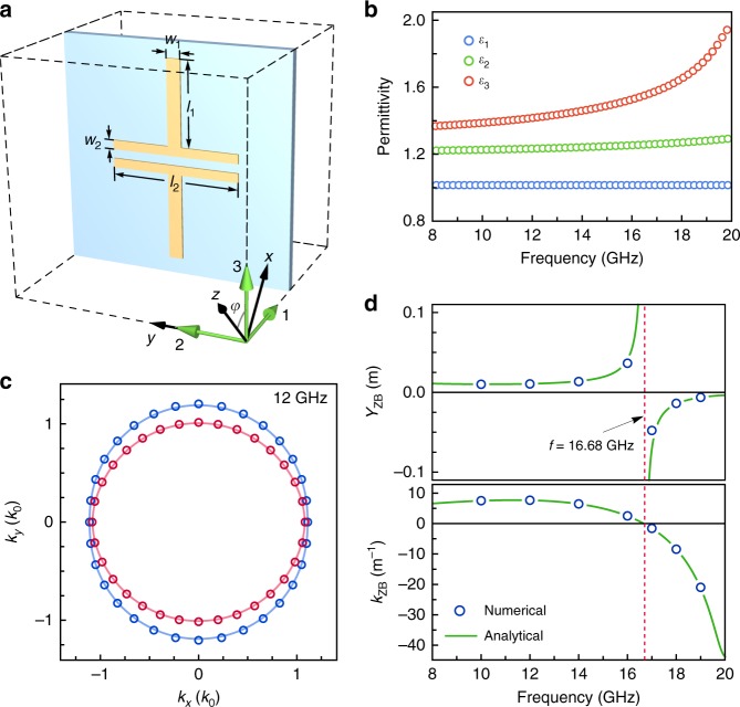
Design of a biaxial metamaterial. a Unit cell of the simple cubic structure with lattice constants d = 5 mm, where a FR4 PCB slab (light blue) with thickness 0.2 mm and relative permittivity fills the coronal plane, and a copper structure of thickness 0.035 mm is printed on the PCB slab with the geometric parameters l1 = 2 mm, l2 = 2.8 mm, w1 = 0.3 mm, and w2 = 0.2 mm. b Dispersions of the retrieved relative permittivities along the three principal axes. c Isofrequency contours of the metamaterial in the xy-plane at 12 GHz, where the circular markers and solid curves correspond, respectively, to the real structure in a and the retrieved homogeneous medium. d Full-wave simulated (blue circles) and analytical (green curves) ZB amplitude YZB and ZB wave number kZB in the homogenized media varying with frequency

