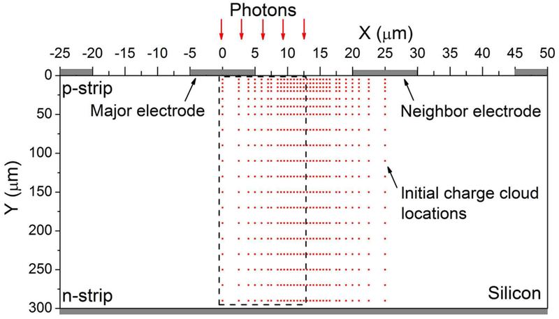
Fig. 2.
Schematic cross section of the DSSSD for TCAD transient current simulation. The simulated device is 300 μm thick with a pitch of 25 μm. The silicon substrate has n-type doping of 5.6×1011 cm−3. The transient currents collected on both the major and neighbor electrodes are calculated. The major collecting electrode is the electrode with a shorter distance from the initial charge cloud compared to the neighboring collecting electrode. Detailed simulation setup can be found from [18].

