
Figure 2.
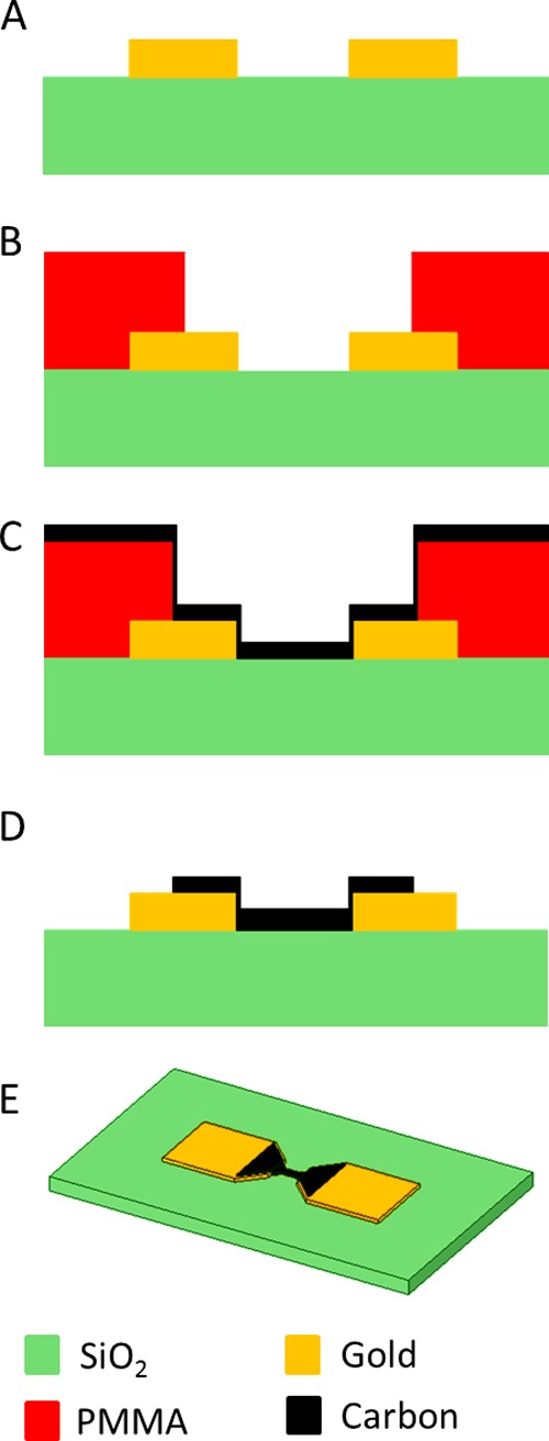
Process flow diagram for the fabrication of thin-film carbon nanofuses on a silicon dioxide film on a silicon substrate with gold contact pads. (A) Gold contact pads with a 5 μm gap are made on a silicon dioxide layer. (B) Poly(methyl methacrylate) (PMMA) is patterned using electron-beam lithography. (C) A 20 nm thin-film carbon layer is deposited by arc deposition. (D, E) A liftoff process leaves a carbon “bow-tie” pattern electrically connected to the gold contact pads.