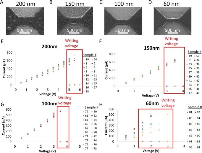
Figure 4.
I–V plots for 73 different thin-film carbon nanofuses with four different widths. (A–D) SEM images of the nanofuses (from left to right) of 17 fuses with 200 nm width, 20 fuses with 150 nm width, 20 fuses with 100 nm width, and 14 fuses with 60 nm width. The scale bars are all 500 nm. The little spheres on the nanofuse in (A) is residual electron-beam resist. It did not affect the testing of the nanofuses. The nanofuses were subjected to increasing voltage until they blew. (E–H) I–V curves of the corresponding thin-film carbon nanofuses. The red boxes illustrate the voltage ranges over which the fuses blow. A voltage below this range did not blow any fuses, whereas a voltage above this range was sufficient to blow all fuses of the noted width.

