Figure 4.
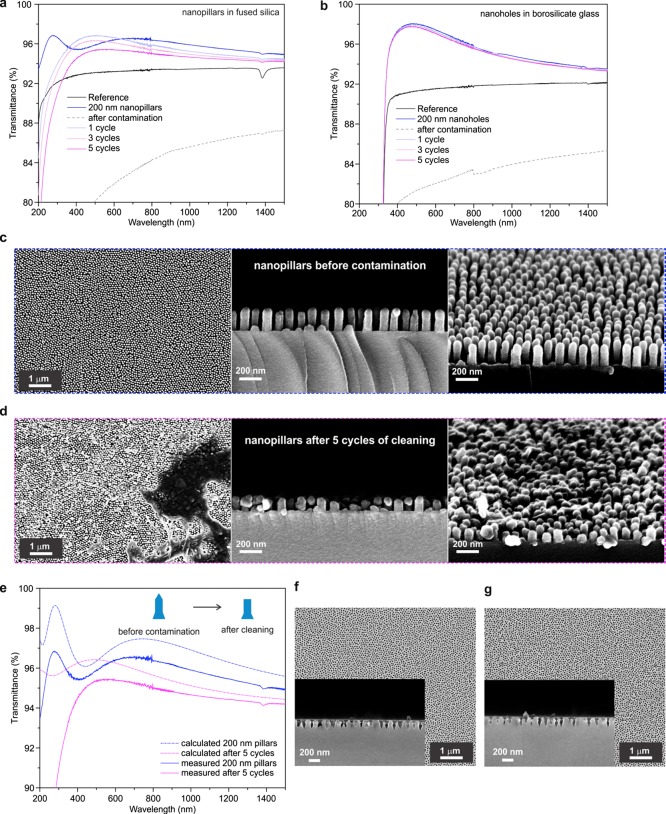
Transmittance of a fused silica nanopillar substrate and a borosilicate nanohole substrate after repeated contamination and cleaning. (a) Transmittance of the fused silica substrate with 200 nm nanopillars on both sides (in blue). The transmittance of the sample after the initial fingerprint contamination (in dashed gray); after 1, 3, or 5 repeated cycles of both fingerprint contamination and cleaning (in light blue, light purple, and purple, respectively). (b) Transmittance of the borosilicate glass substrate with 200 nm nanoholes on both sides (in blue). The transmittance of this sample after the initial fingerprint contamination (in dashed gray); after 1, 3, or 5 repeated cycles of both fingerprint contamination and cleaning (in light blue, light purple, and purple, respectively). (c) SEM images of 200 nm nanopillars before contamination (from left to right: top view, side view, and tilted top view). (d) SEM images of 200 nm nanopillars after five cycles of contamination and cleaning (from left to right: top view, side view, and tilted top view). (e) Measured (solid curves) and calculated (dashed curves) transmittance of 200 nm nanopillars on fused silica before contamination (blue curves) and after five cycles of cleaning and contamination (purple curves). (f) Top-view SEM image of 200 nanoholes before contamination (inset: side view). (g) Top-view SEM image of 200 nanoholes after five cycles of contamination and cleaning (inset: side view).

