Fig. 1.
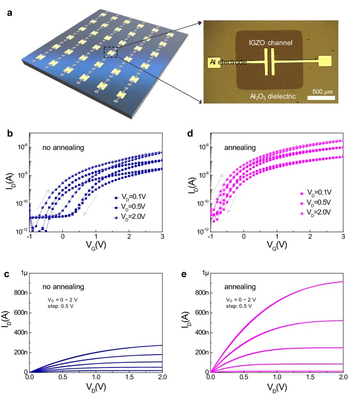
a Schematic of IGZO transistor array devices. The inset shows an optical microscope image of a single IGZO device with a channel region (50 μm length and 500 μm width). Transfer characteristics (drain current–gate voltage of ID–VG) of b reference IGZO transistor without post-annealing and d IGZO transistor with post-annealing at variable VD (0.1, 0.5, and 2 V). Output characteristics (ID–VD) of c reference IGZO transistor and e IGZO transistor with post-annealing at variable VG from 0 to 2 V

