
Figure 9.
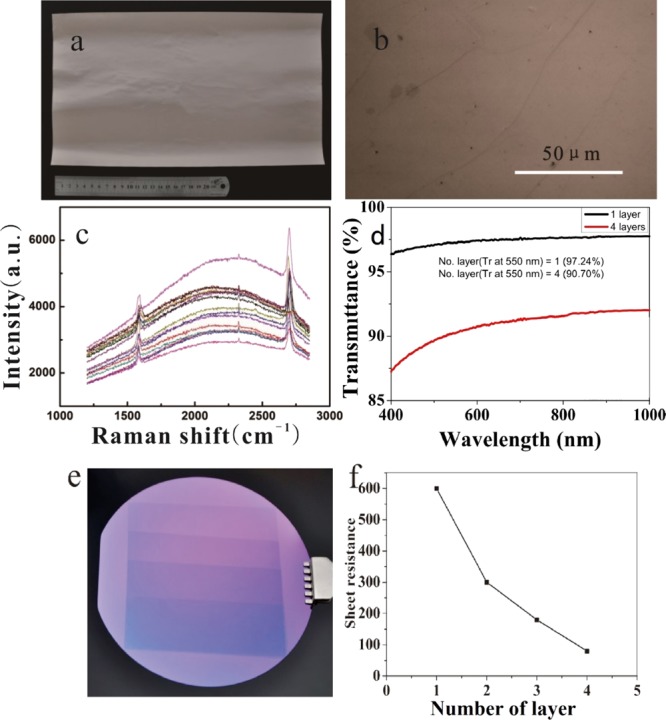
(a) Optical photograph of an as-grown graphene on a oxygen-free copper foil. (b) Microscope photograph of the graphene [the same as in picture (a)] transferred to a silicon substrate. (c) Raman spectra of graphene on a oxygen-free copper foil as shown in figure (a). (d) Transmittance of the monolayer and superposed four layers of graphene film transferred onto the quartz glass sheets. (e) 1–4 layers of graphene film transferred to silicon oxide substrate. (f) Sheet resistance of 1–4 layers graphene film.