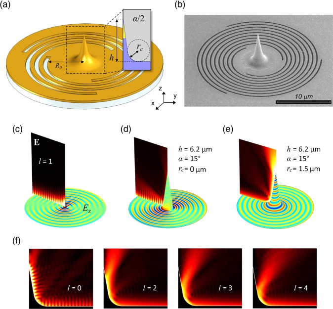
Figure 1.
(a) 3D scheme of the PVL. The geometrical parameters of the spiral slits include a slit width of 200 nm, pitch of 763 nm, gold thickness of 150 nm, and Si3N4 thickness of 100 nm. R0, namely the initial radius of the spirals, is fixed to 4 μm to reduce the effect of direct scattering of light from the grooves. (b) Scanning electron microscope image of an example of fabricated structure. (c–e) |E| maps (vertical cross-section) and Ez maps (metal surface plots) of the central region of the PVLs in the case of a PV impinging with topological charge of l = 1 propagating through a flat PVL center (c), scattered by a conical tip with a zero-basis curvature radius (rc) (d), and by a conical tip with large rc (e). (f) |E| maps in the case of a smoothed conical tip (same parameters as in (e)) illuminated by a PV with the indicated l values.

