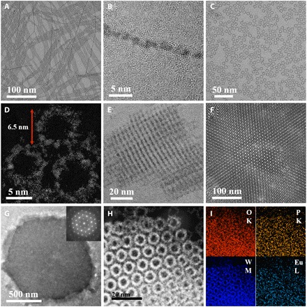
Fig. 2. Characterization of single-cluster nanowires, nanorings, and 3D superstructures.

(A) Typical TEM image of a POM nanowire. (B) High-resolution TEM (HRTEM) image of a single nanowire. (C) Typical transmission electron microscopy (TEM) image of a POM nanoring. (D) High-resolution aberration-corrected TEM image of nanorings. (E) TEM image of a small-size superstructure from the side face. (F) TEM image from the top view of the superstructure. (G) Low-magnification TEM image of a 3D superstructure in large size and the corresponding fast Fourier transform (FFT) image. (H) Dark-field HRTEM image of the superstructure. (I) Energy-dispersive x-ray (EDX) elemental mapping analysis of the superstructure.
