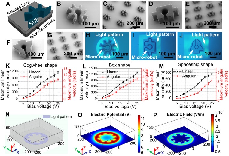
Fig. 1.
Optoelectronic microrobots. (A) Cross-sectional schematic of a cogwheel-shaped microrobot, formed from SU-8 on a sacrificial release layer. (B) SEM image of a cogwheel-shaped microrobot. (C) SEM image of an array of cogwheel-shaped microrobots. (D–G) SEM images of box-shaped and spaceship-shaped microrobots. Bright-field microscope images of (H) a cogwheel-shaped microrobot, (I) a box-shaped microrobot, and (J) a spaceship-shaped microrobot held in place by OET light patterns. Illuminated and nonilluminated regions appear light and dark, respectively. Maximum linear (left axis, black) and angular (right axis, red) velocities as a function of OET bias voltage for translating and rotating (K) cogwheel-shaped microrobots, (L) box-shaped microrobots, and (M) spaceship-shaped microrobots (Movies S1 and S2). Error bars represent ±1 SD from 5 measurements for each condition. (N) Three-dimensional simulation of an OET device in which a light pattern (purple) is projected onto an a-Si:H surface. XY plots at Z = 1.1 μm of simulated (O) electric potential distribution and (P) electric field distribution for a device driven at 20 Vp-p (25 kHz), in which the simulated electric potential and field are indicated in heat maps (blue = low, red = high). The axis dimensions in N-P are in micrometers.

