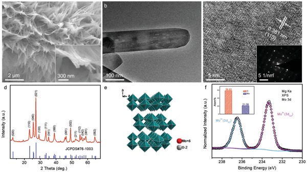
Figure 1.

a) SEM images, b) TEM image, c) HRTEM image, d) XRD pattern, e) layered crystal structure, and f) core‐level Mo 3d of XPS spectrum of the MoO3 nanowires. The insets in (c,f) are its corresponding SAED pattern and the atom% of Mo and O, respectively.
