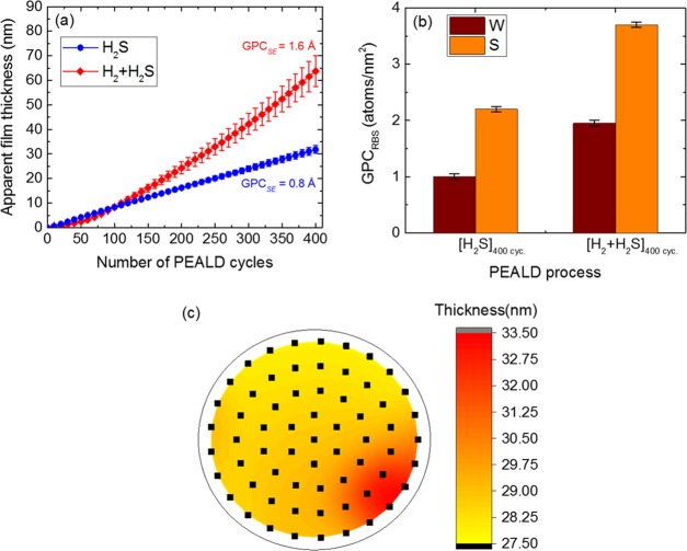
Figure 1.
(a) Apparent film thickness (tApp) as a function of number of PEALD cycles for the H2S and H2 + H2S processes at a deposition temperature of 300 °C, as determined from in situ SE measurements. The error bars are a cumulative sum of the measurement error and SE model fitting error. (b) GPCRBS (atoms/nm2) in terms of number of deposited W and S atoms showing an analogous trend as GPCSE for the H2S and H2 + H2S processes. GPCRBS was determined after 400 PEALD cycles. (c) Thickness uniformity map of WS2 films (H2S process) on a 4 in. SiO2/Si wafer, as determined from room-temperature ex situ SE measurements. The black squares on the wafer represent the SE measurement points with a 5 mm edge exclusion.

