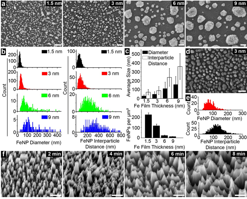
Figure 2:

Preparation of FeNP coated surface for nanostructure fabrication. a) FeNPs of various sizes and inter-particle distances formed from iron film with various thicknesses. Scale bars are 100 nm. b) FeNP size and inter-particle distance distribution in each film thickness. c) quantitative analyses of average FeNP size and inter-particle distance (top), and density of FeNPs for each film thickness (bottom). (Top) Error bars are standard deviation of average nanoparticle size across respective figures of 2a. Large error bars are a result of size distribution. (Bottom) Error bars are standard deviation of 5 square area density across respective figures of 2a. d) SEM image (top view) of FeNPs formed under 4% hydrogen. Scale bar is 200 nm e) quantitative analyses of the average size of FeNPs and inter-particle distance formed under 4% hydrogen. f) generated nanostructures after etching for 2, 4, 6, and 8 min. Scale bars are 200 nm.
