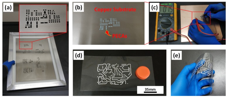
Figure 6.
(a) Stencil printing mask prepared by laser beam cutting with the thickness of 100 μm; (b) Stencil printing PECA patterns corresponding to the mask on the copper substrate playing the same role as Sn-Pb solders pastes; (c) Photographs of the relative resistance of the PECAs after curing; (d,e) Photographs of printable flexible circuits on a PET film. The printed circuits still maintained excellent adhesion performance during the bending process.

