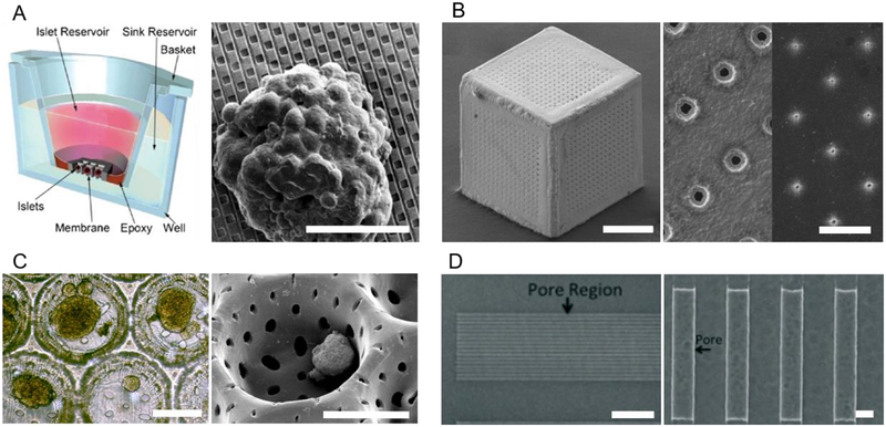
Fig. 5: Pore Configurations in Cell-Seeded Substrates.
(A) Schematic (left) of NanoGland device and scanning electron microscopy image (right) of islet seeded at the bottom of a sample well, rectangular nanopores in silicon substrate, fabricated by a sacrificial layer technique, shown in dark gray (adapted with permission from [267]; scale bar: 40 μm). (B) Scanning electron microscopy images of gold cell encapsulation device (left; scale bar: 200 μm), and close-up of pore structure (right; scale bar: 10 μm); pore size varied by modulating gold deposition time atop a substrate (adapted with permission from [273]). (C) Light-microscopy (left) and scanning electron microscopy (right) images of islets within poly(ethylene oxide terephthalate)/poly(butylene terephthalate) copolymer porous wells. Pores were forged by laser drilling (adapted with permission from [283]; scale bars: 200 μm). (D) Scanning electron microscopy images of nanoporous region of silicon nanopore membrane (left; scale bar: 20 μm), and close-up of rectangular pore structure (right; scale bar: 300 nm), fabricated by micro-electromechanical systems technology (adapted with permission from [296]).

