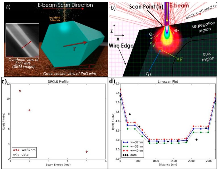
Figure 6.
(a) Illustration of the line-scan CLS measurement process and SEI picture of a typical electron beam track across the ZnO wire diameter. (b) Illustration of electron-hole pair creation geometry and geometric parameters used for the defect profile simulation. (c) Single spot depth dependence measurement of I(defect)/I(NBE) intensity ratio versus incident beam energy EB. (d) 5 keV line-scan data (black dots) and best fit (blue line and dots) showing defect emissions extending nearly 1000 nm into the microwire bulk. Reprinted with permission from the Royal Society of Chemistry [15].

