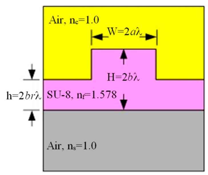
Figure 9.

Cross section of the waveguide structure showing the geometric parameters and optical properties of the materials in each layer.

Cross section of the waveguide structure showing the geometric parameters and optical properties of the materials in each layer.