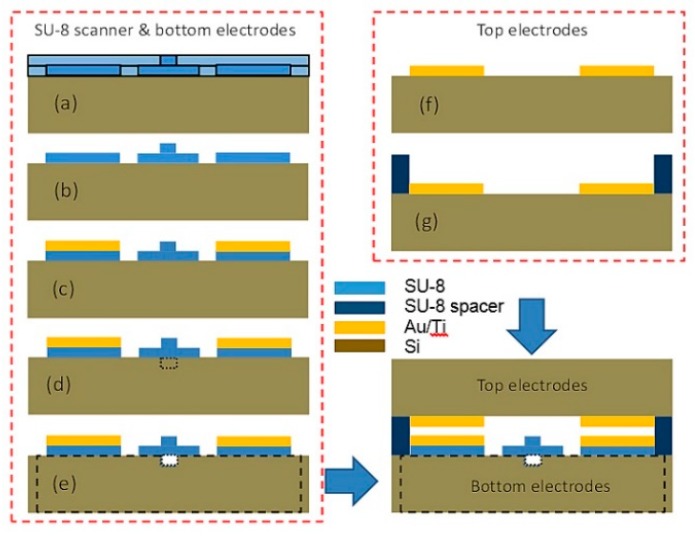
Figure 13.
Fabrication process of electrostatic scanner. (a–e): scanner body and bottom electrodes (f,g): top electrodes. (a) Double-layer photolithography process to define rib shape waveguide and scanner pads; (b) Development process to create SU-8 waveguide and body; (c) Au/Ti thin films are deposited and patterned by lift-off process; (d) Front side fiber grooves are patterned and deep etched using deep reactive-ion etching (DRIE); (e) the scanner (bottom electrode and waveguide) were released by DRIE again from the backside of the wafer; (e) Backside etch-through to release actuators and waveguide; (f) top electrode is deposited and patterned on a second silicon wafer; (g) SU-8 spacers are spun and patterned.

