Fig. 1.
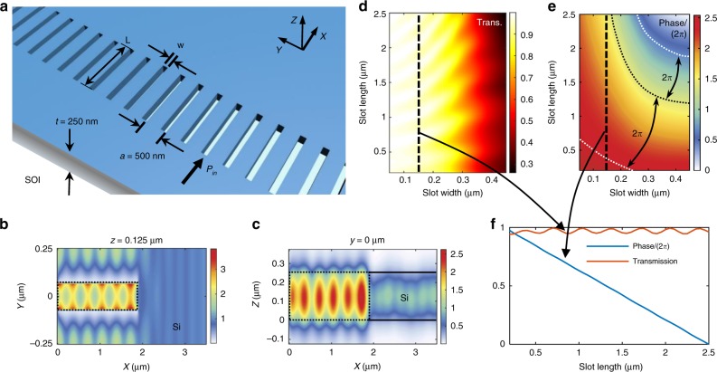
The design principle of low loss on-chip HCTAs. a A schematic view of 1D HCTA with a lattice constant a = 500 nm, defined on SOI substrate. It can impose localized phase shift on the electromagnetic wave traveling in plane. b Typical top (x–y plane) and c side (x–z plane) view of the intensity profile |Ey|2 near the air slot. The dotted lines show the outline of the slot and the solid lines show the outline of silicon slab. d Simulated amplitude and e phase retardation of the transmission as a function of the slot width and length. The wavelength of the input light is 1550 nm. f The simulated amplitude and phase of the transmission versus slot length, fixing the slot width to be 140 μm

