Fig. 2.
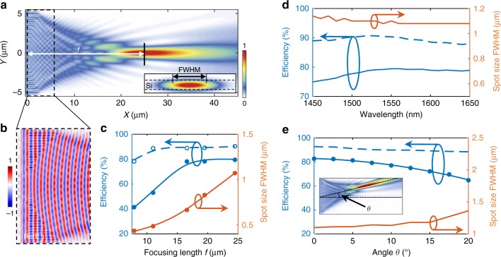
HCTA based on-chip metalens. a In-plane light distribution of |Ey|2 in the middle of the silicon slab with incident light parallel to its optical axis. Inset: cross-sectional view of the light distribution on the focal plane, with the minimal spot size marked as FWHM. b Simulated electric field distribution, Ey, in the region highlighted by a dashed box in a. c Simulated focusing efficiency (solid dots), transmission (empty circles) and FWHM versus focal length as marked in a. The curves are eye guides. The lens dimension is fixed at 10 µm with varying lens design. d Focusing efficiency, transmission and the FWHM of the metalens with a focal length of 25 μm. e Focusing efficiency, transmission and the FWHM of the metalens with a focal length of 25 μm at oblique incidence angle from 0o to 20o. Inset: In-plane light distribution of |Ey|2 at an oblique incident angle of 7.5°

