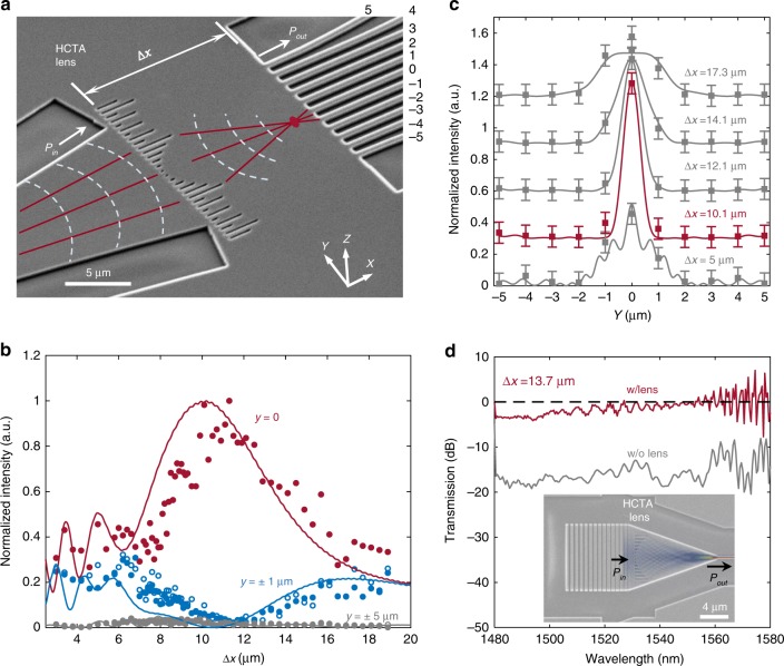
Fig. 3.
Demonstration of on-chip low loss metalens for ultracompact taper. a Scanning electron microscope (SEM) image of an on-chip metalens with a focusing length of 8 μm, object distance of 44 µm, and image distance of 10.1 μm. Eleven single mode waveguides are placed on the output plane for mapping the spatial distribution of light. b Comparison of the simulated (solid lines) and measured intensity profile (filled and empty circles stand for the positive and negative coordinates respectively) along the optical axis. c The mode profile evolvement with Δx, and the black line is the profile at the focusing plane. The error bars represent the standard deviation (s.d.) for three measurements. d Transmission spectra of a 13.7-μm-long taper with and without metalens, after normalization to a grating coupler with a 250-μm long taper. Inset: SEM image of the ultracompact metalens taper connecting a grating coupler (width of 11 μm) and single mode waveguide (width of 0.5 μm) superimposed with the simulated intensity distribution

